Osman Sibonjic from the Institute of Metrology of Bosnia and Herzegovina (IMBIH) has successfully completed a 3 months Research Mobility Grant (RMG) programme under the framework of the European Metrology Programme for Innovation and Research (EMPIR) as part of the project “RF measurements for future communications applications – 20IND03 FutureCom“. Osman was at the National Physical Laboratory (NPL), UK from 19th April 2022 to 15th July 2022 and during this period he carried out the following research tasks with support from NPL:
- Task 1: HF PCB design and real-world simulation
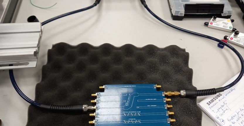
In this task RMG researcher participated in designing, fabricating, and testing Printed Circuit Boards (PCBs), with support from NPL, so that signal integrity effects can be evaluated. Different structures are considered with the aim to achieve appropriate signal integrity. 1–port and 2-port devices with specific characteristics of S parameters are designed on PCB board (Through, 3 dB Attenuator, Beatty line, Short circuits, Offset short circuits, Matched loads, etc.). Signal integrity of the mentioned structures is simulated using Quite Universal Circuit Simulator (QUCS) with support from the NPL. Simulations are realized using input technical parameters for microstrip lines and substrates (length and width of the lines, relative permittivity, diameter via, substrate loss tangent, etc.) from the process of PCB design and fabrication.
- Task 2: Testing of the manufactured PCB using a VNA, and comparing results to the real-world simulations
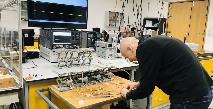
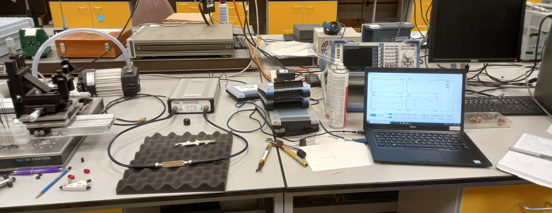
In this task RMG researcher with support from NPL trained to use VNAs PicoVNA (8.5 GHz) and Keysight PNA N5222B (26.5 GHz), tested and measured S parameters for the integrated devices on the HF PCB using PicoVNA in order to establish overall electrical performance and evaluate signal integrity. Measurement results of S parameters acquired by calibrated VNA using the SOL calibration scheme represented typical electrical performances for integrated 1-port and 2-port devices on PCBs.
These results are compared with results from simulations using the software mentioned in task 1. Simulated results correspond to the results received from the real measurements that represent typical responses for integrated devices on the manufactured PCBs.


